Vapor Deposited Nano-Coatings vs NanoSlic Gold – Gathering Data

Blog by Greg Smith, Manager of Stencil Technology at BlueRing Stencils
Vapor Deposited Stencil Nano-Coatings – A New Break Thru or Just Another Coating?
I presented this paper at SMTA International 2023 last fall. It was the initial work we did to collect the data needed to determine how vapor deposited Nano-Coatings performed vs our current Nanoslic Gold stencil coating. If you missed this presentation and paper, both are available on our website at https://blueringstencils.com/documents/.
If you don’t have time to go back and read it, I would like to summarize the paper and our findings in this short blog.
What are Vapor Deposited Nano-Coatings?
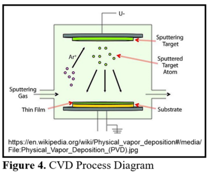
Wikipedia defines Chemical vapor deposition (CVD) as “a vacuum deposition method used to produce high-quality, and high-performance, solid materials. The process is often used in the semiconductor industry to produce thin films. In typical CVD, the wafer is exposed to one or more volatile precursors, which react and/or decompose on the substrate surface to produce the desired deposit.”
Basically, the process consists of “Targets” or “Precursors” comprised of proprietary materials that rotate in the chamber with the stencils to be coated. Once heat and vacuum are introduced, oxidation takes place, and these materials are vaporized and redeposited onto the stencil foil. The vapor deposited materials create layers of color and coatings to create a proprietary hydrophobic and oleophobic nano-coating.
How did we do this research?
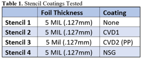
Four stencils were used for this experiment. All stencils were 5 mil Fine Grain (less than 5 micron grain stucture), stainless steel foil. All stencils were laser cut using the same program/laser and mounted on 29×29 spacesaver frames. CVD indicates Chemical Vapor Deposition and NSG indicates Nanoslic Gold in the data. (PP) indicates a Plasma Polish process. The only difference in each stencil was the stencil coating which is shown below:
Why did we decide to test two different types of Vapor Deposited Coatings?
When the initial stencil arrived with the Vapor Deposited Coating, I noticed electrical contact marks similar to those seen on “electro-polished” stencils. This electro-polishing process has not been used by mainstream stencil manufacturers in the United States for several years because of the cut quality of modern laser systems used to cut stencils. In addition, I noticed a masked area around the stencil apertures that looked somewhat polished. I asked the company that did the coating and found out that the process used was not “electro-polishing” but was a “plasma-polishing” process. Immediately, I requested an additional stencil to be coated with the vapor deposition process without the plasma-polish process so that we could get independent testing with the different variables involved in the process. This additional stencil became our Stencil2, CVD1 with no plasma polish. Stencil3, CVD2 (PP) was the same CVD process with plasma polishing.
What did we measure in our data and why?
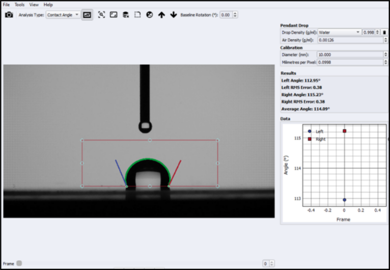
With all nano-coatings there are a few key areas to look at once the data is collected. The first is a measure of how much the coating repels water and oil based chemistry (hydrophobic and oleophobic). This is called contact angle and is measured by a device called a Goniometer. It measures the angle between the bottom of the chemical droplet and the surface of the coated stencil.
The second area we looked at was coating thickness. This was just to understand the differences in the coatings and to determine potential wear challenges.
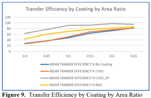
The third and one of the most important areas to evaluate was transfer efficiency of the coating. Transfer efficiency is a measure of how well the solder paste releases from the stencil apertures and is calculated as the volume of paste deposited onto the PCB land pad divided by the theoretical paste volume that would fill the stencil aperture, It is expressed as a percentage. As component miniaturization continues to evolve in our industry, we must be able to print solder paste through apertures with lower area ratio’s.
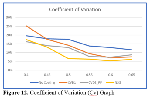
The final area that we investigated, perhaps the most important, is the Coefficient of Variation. This is a key indicator in the effectiveness of stencil coatings specifically when looking at thin foil apertures that have very low area ratios. It is calculated as the standard deviation of a population divided by its mean. Applied to solder paste deposits, CV represents the spread of the volume, height, area or offset data. Because the average volumes of solder paste deposits vary based on many input variables, basic standard deviations should not be used to evaluate different distributions of data. Expressing the variation as a percent of the average normalizes it for better comparison. Continued component miniaturization requires not only exceptional solder paste release but also very controlled process repeatability.
Here is the data we collected:
Coating Contact Angle:
Coating Thickness:
Transfer Efficiency:
Coefficient of Variation:
Summary: What does the data tell us:
The chemical vapor deposited nano-coatings tested offered improved transfer efficiency if plasma polishing is done prior to the application. Without the plasma polishing process, the coating was no better than an uncoated stencil indicating improved transfer efficiency of the CVD coating comes from the plasma polish process. The vapor deposited coating without plasma coating did show improved contact angles vs an uncoated stencil, but again, the transfer efficiency was not improved. Based on the coefficient of variation percentages, the smallest area ratio to use this vapor deposited coating and maintain value in the good zone (under 10%) is 0.55. Nanoslic Gold values were good at 0.50 area ratio.
When comparing coatings, I always look at both transfer efficiency and coefficient of variation. The CVD with plasma polish created higher transfer efficiency numbers than Nanoslic Gold but the coefficient of variation percentages of Nanoslic Gold were better. With this information, I’m confident in saying the CVD coating tested was not better than our current Nanoslic technology for overall stencil performance. In addition, the CVD coating process is a much more expensive process than the Nanoslic Gold process. For the higher price typically associated with Chemical Vapor Deposited stencil coatings, I would expect to see significant improvement in both transfer efficiency and coefficient of variation. At this point, there is no significant improvement for the cost difference required.


